CAS Latency, theoretical performance and safe RAM voltages
21 December 2023Latest modification: 22 December 2023
RAM latency
RAM latency is another basic parameter that directly affects module performance. As in the case of clocking, it counts the highest possible value, so in the case of latency, it counts the lowest possible value.
Seeing numbers such as CL34-44-44-78 1T in the module specifications, it is useful to know what they mean. These values relate directly to CL-TRCD-TRP-TRAS and CR. All the listed values are calculated in clock cycles.
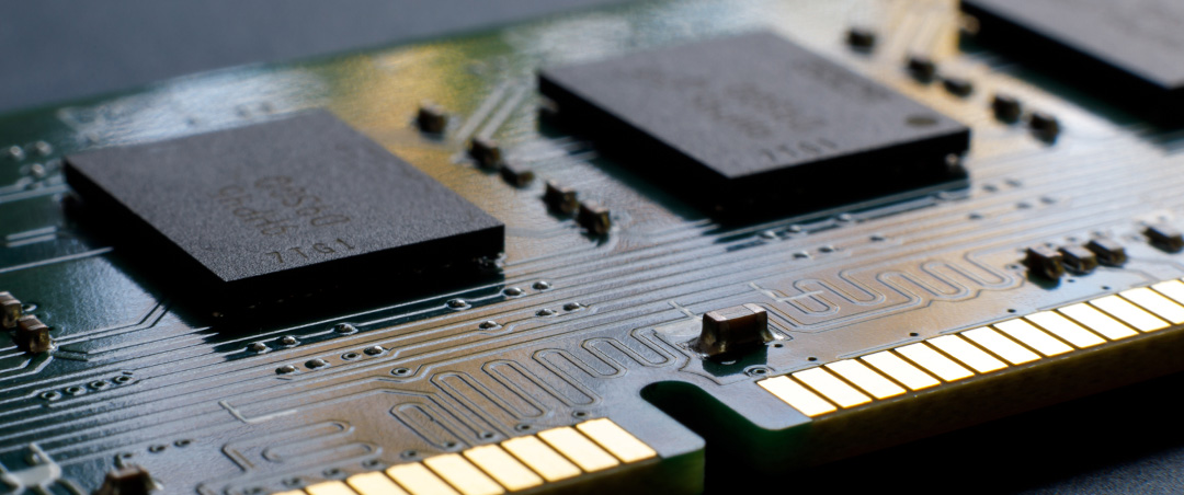
CL (CAS Latency) – is the number of clock cycles that must pass between receiving a request to access a column of DRAM until the data is exposed on the bus.
tRCD (Row Address to Column Address Delay) – determines the minimum number of clock cycles from the time a row of memory is addressed until columns are accessed. The time to read the first word from memory requiring addressing a row is tRCD+CL clock cycles.
tRP (Row Precharge Time) – determines the minimum number of clock cycles that must elapse from the time of closure to address the next memory row in the same bank. If a row needs to be changed, the access time to the next row is tRP+tRCD+CL clock cycles.
tRAS (Row Active Time) – determines the minimum number of clock cycles that must elapse between the activation of a row and its closure.
CR (Command Rate) – determines the time in clock cycles during which a row or column address is issued on the signal lines. A value of 1T says that the address on the signal lines is available after one clock cycle, while 2T says that two full clock cycles must occur. The higher the CR number, the higher the latency. The CR value depends on the modules clock frequency and its design (e.g. Single Rank or Dual Rank). The higher the clock rate, capacity, and level of complexity of the module design, the more advisable is the 2T value.
Theoretical performance of memory modules
The relationship between speed (MT/s) and latency (CL) can be compared to moving on different highways at one time. Assuming that we are given “access” to a highway for a certain period of time which is specified in CL, then we can make movement on a particular highway at a certain speed expressed in MT/s. Due to the very large number of operations performed in the computer during one second, then the change of the example highway is very frequent, so that the overall performance is affected by the response time and access to the highways themselves (memory bits), as well as the speed of movement on them.
Knowing that for the actual performance of RAM it is not only speed that matters, but also low latency, then you can calculate the theoretical performance of modules by substituting the values of a specific memory into the formula.
(1 / [(MT/s) / 2] x CL) x 1000
Taking 6400 MT/s and CL34 latency as an example, we can calculate the approximate response time of the example modules, which will be expressed in nanoseconds (ns).
(1 / [6400 / 2] x 34) x 1000
(1 / 3200 x 34) x 1000
0,010625 x 1000
10,625 ns
When we substitute slightly faster 6800 MT/s modules into the same formula, but with significantly increased latency at CL40, the result is approximately 11,765 nanoseconds, so the response time compared to 6400 MT/s CL34 modules is more than 1 nanosecond longer. As a reminder, a nanosecond is one billionth of a second, and even in such a short time more than a few million operations can be performed. Therefore, every part of a nanosecond directly translates into the overall performance of the modules and the entire computer.
RAM module operating voltages
DDR5 memories operate at voltages of 1.1 V, which is 0.1V lower than its predecessor. Such voltages affect lower power consumption, but you need to know that this applies only to modules whose operating parameters are nominal and result from the components used, compliant with the JEDEC standard, in other words – not overclocked.
For higher-performance modules, otherwise known as “OC” (overclocked), the voltage value must be raised. To achieve even higher performance in DDR5 modules, the voltages go up to the same magnitudes as in the previous generation. Voltages in the latest generation of overclocked modules range between 1.25 and 1.45 V. The specified voltages are safe ones, and it is not recommended to exceed them, as this can affect the stability of the entire computer or lead to damage to the modules themselves or even the motherboard.

If the saved overclocking profile has an assigned value of 1.35 V, it is worth raising the voltage minimally (in this case by 0.1 V) and rechecking the stability of operation of the modules with increased clock speed or lowered latency. If the expected stability is not achieved, it remains to reduce the aforementioned speed or increase the latency.
We hope that our series of three materials on RAM has helped to familiarize you with the principle of operation of even individual elements of RAM, making it easier to understand how they work in your computer. Each memory is a collection of many parameters that directly interact with each other.
When choosing your memory modules, you need to pay special attention to capacity, speed, and latency (CL) – you’ll learn about everything in this and the previous two materials 🙂
Now it’s high time to provide some more details about SSDs and NAND memory! There will be more on this topic in future articles, so stay tuned for more of our material 😉
If you want to check out our other materials then please visit our blog HERE.
Do any questions come up? Have we made a mistake somewhere or do you want to add something? Write to us at marketing@goodram.com or Facebook – GOODRAM/IRDM.
